The new 40,000-square-foot facility expands HCLTech’s semiconductor engineering capabilities with advanced testing, validation and failure-analysis infrastructure, supporting chipmakers across R&D, pre-production and production qualification in India and overseas.
HCLTech has strengthened its semiconductor engineering capabilities with the launch of an Advanced Semiconductor Lab in Bengaluru, backed by an investment of Rs 185 crore. The facility is aimed at supporting the growing requirements of chip companies for post-silicon engineering, testing, validation and failure analysis as India expands its presence in the global semiconductor ecosystem.
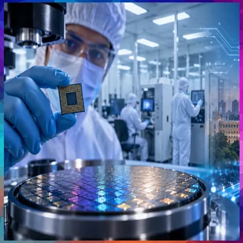
Spread across 40,000 square feet, the facility includes 25,000 square feet of Class 10K and Class 1K cleanroom infrastructure. It is designed to serve semiconductor customers through multiple stages of the product lifecycle, covering research and development, pre-production activities and production qualification.
The Bengaluru lab brings together advanced testing and measurement equipment from technology providers including Teradyne, Advantest, Keysight, Tektronix and Thermo Fisher Scientific. HCLTech said integrating these capabilities at a single location will help customers streamline testing workflows and potentially reduce turnaround times.
Integrated platform targets semiconductor testing needs
The new facility builds on HCLTech’s nearly two decades of experience in semiconductor engineering and is aligned with its Spec2Parts business model. The model combines electrical validation, automated testing, qualification and failure analysis within an integrated service framework.
By bringing these functions together, HCLTech aims to reduce the complexity involved in managing different stages of semiconductor testing through multiple service providers. The facility is expected to support both Indian and international customers seeking engineering and qualification capabilities closer to their development and production cycles.
“The inauguration of our Advanced Semiconductor Lab in Bengaluru is a proud milestone for HCLTech and reinforces India’s growing leadership in semiconductor innovation. This facility reflects our deep commitment to investing in high-end engineering capabilities. We are excited to contribute to the country’s vision of becoming a global hub for advanced technology,” said Hari Sadarahalli, Corporate Vice President and Global Head, Engineering and R&D Services at HCLTech.
The lab's infrastructure includes automated test equipment, semiconductor probing systems, qualification chambers and advanced failure-analysis tools. These include optical and electron microscopy systems as well as focused ion beam (FIB) equipment, enabling detailed examination and analysis of semiconductor devices.
Facility to pursue global quality certifications
HCLTech said the facility is also set to pursue several international certifications, including ISO 17025 and ISO 9001, along with AS 9100 for the aerospace and defence sector and ISO 13485 for medical applications.
The company expects the facility to address an important requirement within India's semiconductor ecosystem by providing integrated testing and validation capabilities. As chip development increasingly requires specialised post-silicon analysis and qualification, such infrastructure can help semiconductor companies shorten development cycles and identify issues before products move further into production.
With the Bengaluru lab, HCLTech is expanding its ability to support semiconductor companies across India and international markets. The investment also reflects the broader industry push towards building domestic capabilities across the semiconductor value chain, beyond chip design and fabrication to include testing, validation and reliability engineering.